
File:Pad Cratering 02.jpg
No higher resolution available.
Pad_Cratering_02.jpg (387 × 292 pixels, file size: 10 KB, MIME type: image/jpeg)
| This is a file from the Wikimedia Commons. Information from its description page there is shown below. Commons is a freely licensed media file repository. You can help. |
Summary
| Description |
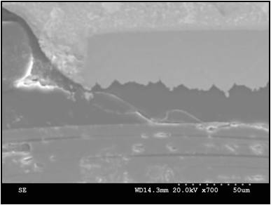
English: Magnified view of cross section of BGA pad and solder ball. Dielectric has cracked and starting the pad to lift. Eventually creating pad cratering. |
| Date | |
| Source | Integral Technology, Lake Forest, CA |
| Author | Chris Hunrath |
Licensing

|
The copyright holder of this file allows anyone to use it for any purpose, provided that the copyright holder is properly attributed. Redistribution, derivative work, commercial use, and all other use is permitted. |
|
|
File history
Click on a date/time to view the file as it appeared at that time.
| Date/Time | Thumbnail | Dimensions | User | Comment | |
|---|---|---|---|---|---|
| current | 00:43, 9 November 2010 | | 387 × 292 (10 KB) | Rockyh2 | {{Information |Description={{en|1=Magnified view of cross section of BGA pad and solder ball. Dielectric has cracked and starting the pad to lift. Eventually creating pad cratering.}} |Source=Integral Technology, Lake Forest, CA |Author=Chris Hunrath |Dat |
File usage
The following pages on the English Wikipedia use this file (pages on other projects are not listed):